

Materials Development Towards an Energy-efficient Spintronic Logic Device

Author(s)
Jia-Yeh WangBiography
Jia-Yeh Wang, PhD, Purdue University, West Lafayette, and MS of Aero from NCKU. He has successively served as the CEO of GLORIA and Dean of EOOIA, CYCU, EVP and Managing Director of Paragon Technologies (3518), EVP of ARX, Head of IE, JSUST, Researcher of the Aerospace Center of ITRI, Seradyne (USA), and Mfg. R&D Center in The Torrington Co. (USA). He has expertise in precision manufacturing, electronic heat transfer, precision ceramics, functional and optical vacuum coating technologies, etc. In almost all stages in his career, he was in charge of leading new technology and new business development. Last year, at the invitation of Mr. Ken Tai, the co-founder of Acer, he joined his team, built and led the Digital Optics Development Center (DODC), which is aimed at paving the way to link Digital Optics with digital electronics and AI.
Academy/University/Organization
Digital Optics Development Center-
TAGS
-
Share this article
You are free to share this article under the Attribution 4.0 International license
- ENGINEERING & TECHNOLOGIES
- Text & Image
- April 14,2021
In recent years, advanced countries in the East and the West have successively proposed development routes and policy guidelines for the profound importance of the digital transformation of photons and optics in the future development of science and technology. Under the trend of digitization, informatization, programmability, and miniaturization, digital optics has been developed based on X-on-CMOS with wave optics, technologies of semiconductors, array-based materials, IC design, driving, and software to provide industry, academia, and the research community with a new optical tool and platform that breaks through the limitations of the structure of traditional optics. It also leads to the integration of digital electronics and AI. The core technology and concepts of Digital Modulation and FPLA, respectively, provide unprecedented superposition and parallel processing capabilities. Digital optics proactively controls and tunes the light source and light field, and simplifies the system by its programmability while increasing the flexibility, speed, and functionalities so as to open the gate for industry, technology innovation, applications, and more possibilities.
The progress of tools has brought about the growth of technology. Good optical systems allow us to observe the world more precisely, which leads to the progress of science. The advancement of technologies, in turn, leads to the development of new ideas and possibilities for optics. The new optics further promote the innovation and application of technology. For decades, optical innovations and applications have entered our lives and every sector of industry. In recent years, from Horizon 2020 in Europe, Advanced Manufacturing Partner 2.0 in the US, and Japan's optoelectronics to topological quantum strategy projects, each has proposed development routes and policy guidelines for the importance of photonics- and optics-related technologies. In the past two years, SPIE has also emphasized the key role of photonic technology and optical digital transformation in the future development of technology and industry. The trends of digitization, informatization, programming, and miniaturization have led the development of optics by integrating more material technologies into the development context and foundation of digital electronics, semiconductors, and IC design technologies so as to better use and control the light and implant it in various industry segments.
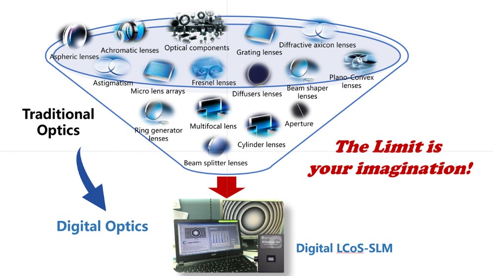
The journey and achievements of semiconductors and digital electronics have provided a very similar development path for digital optics. The rapid advancement of miniaturization and the order of magnitude of transistors have foreshadowed more possibilities and imagination for the development of digital optics (Figure 1). The realization of optical digitization is based on cross-field technologies such as geometric and physical optics, semiconductors, liquid crystals, IC design, driving, and software. It provides limit-breaking optical tools and platforms that bridge digital electronics and AI (Figure 2), and opens the gate for industry, technology innovation, applications, and new possibilities.
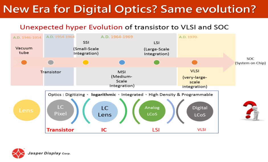
Figure 1: Digital Optics follows a similar path to that of Digital Electronics
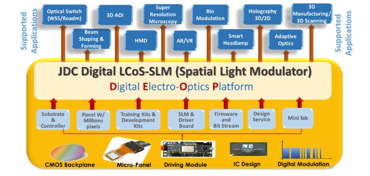
Figure 2: Digital Electro-Optics Platform: the basis for Digital Optics
The importance of digital optics manifests itself in the ability to proactively master and manipulate the light in optical systems, from particle-based geometric optics to wave- and phase-based physical optics, from traditional optics by reflection and refraction, to diffraction and Fourier optics. Following the concept of X-on-CMOS and based on the heterogeneous integration of semiconductor and liquid crystal, optics has been transformed from the 3D lens into its planar, 2D equivalent micro-optical counterpart. With the matured theory of physics and mathematics infused into the framework of digital electronics, operated in a digitally driven environment with software-based UI, optic systems are greatly simplified, while the complexity and the threshold of learning and operating are also effectively reduced.
The JDC's core component of digital LCoS-SLM uses a digital structure array of millions or even tens of millions of pixels, with key digital modulation technology (Digital Modulation). Analogous to the FPGA concept, the feature of binary control on the pixel-level forms the idea of FPLA (Field Programmable Light/Lens Array) that presents excellent superposition and parallel processing capabilities. Different from the passive nature of image processing, FPLA operates proactively on the light source and light field with its programmability, effectively simplifying the system and increasing the flexibility, speed, and functionalities. Digital optics greatly reduces the pain and load of the design and the adjustment of the light path and system of traditional optics, and therefore serves as the wing for the relaunching of optics!
The development of digital optics is just about to begin. More professionals, field experts, and young students are urged to participate and devote themselves to learning and research to accelerate the process of digital transformation and development of optics. Therefore, more and concrete contributions to adding value to and upgrading various industries can be anticipated. Vivid testimonials from university physics teachers participating in a 3-day digital optics immersion course held by the American Association of Physics Teachers (AAPT) and the Advanced Physics Laboratory Association (ALPhA) included: "I've just seen the future of optics" and "The future of optics is programmable" (Figure 3)!
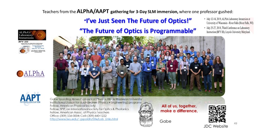
Figure 3: Testimonials of physics teachers after a 3-day immersion course
RELATED

STAY CONNECTED. SUBSCRIBE TO OUR NEWSLETTER.
Add your information below to receive daily updates.