

Mobile 5G enables smart living and digital economic development

Author(s)
Chih-Chao YangBiography
Dr. Chih-Caho Yang is currently an associate researcher in chip integration technology division of Taiwan semiconductor research institute. His research interests include the development of monolithic 3D integrated circuit and advanced 3D device for artificial intelligence and internet of things.
Academy/University/Organization
Taiwan Semiconductor Research InstituteSource
Chih-Chao Yang, Tung-Ying Hsieh, Po-Tsang Huang, Kuan-Neng Chen, Wan-Chi Wu, Shih-Wei Chen, Chia-He Chang, Chang-Hong Shen, Jia-Min Shieh, Chenming Hu, Meng-Chyi Wu, and Wen-Kuan Yeh, IEEE International Electron Devices Meeting (IEDM), 2018.
Ping-Yi Hsieh, Yi-Jui Chang, Pin-Jun Chen, Chun-Liang Chen, Chih-Chao Yang, Po-Tsang Huang, Yi-Jing Chen, Chih-Ming Shen, Yu-Wei Liu, Chien-Chi Huang, Ming-Chi Tai, Wei-Chung Lo, Chang-Hong Shen, Jia-Min Shieh, Da-Chiang Chang, Kuan-Neng Chen, Wen-Kuan Yeh, and Chenming Hu, IEEE International Electron Devices Meeting (IEDM), 2019.-
TAGS
-
Share this article
You are free to share this article under the Attribution 4.0 International license
- ENGINEERING & TECHNOLOGIES
- Text & Image
- April 22,2020
The “More than Moore” monolithic 3D integration approach, which is nearly compatible with today’s semiconductor process, is one of the most promising ways to achieve high density, high-performance, rich-function, energy-efficient, and low-cost integrated circuits that meet the requirements of AI and IoT chips. Laser recrystallized poly-Si channels for monolithic 3D device fabrication have the benefits of being simple and low cost. The laser process provides an ultra-shallow heating and recrystallization process which prevents damage. The only concern is the electrical property variation caused by defects and grain boundaries in the poly-Si channel for circuit design.
TSRI’s monolithic 3DIC research team aims at manufacturing advanced monolithic 3D devices and related functional units using green nanosecond laser recrystallization. We proposed a back-end of line (BEOL) location-controlled-grain (LCG) technique for manufacturing high performance monolithic 3D integrated circuits in collaboration with NCTU and NTHU research teams for AI and IoT application. Using the LCG technique, we have obtained a regularly patterned array of single-grain Si matrix, which allows the fabrication of FinFETs and circuit units without grain boundaries. It shall dramatically improve the semiconductor chip performance and production yield. This advanced M3D research service platform welcomes collaboration with the industrial, academic and research sectors in Taiwan.
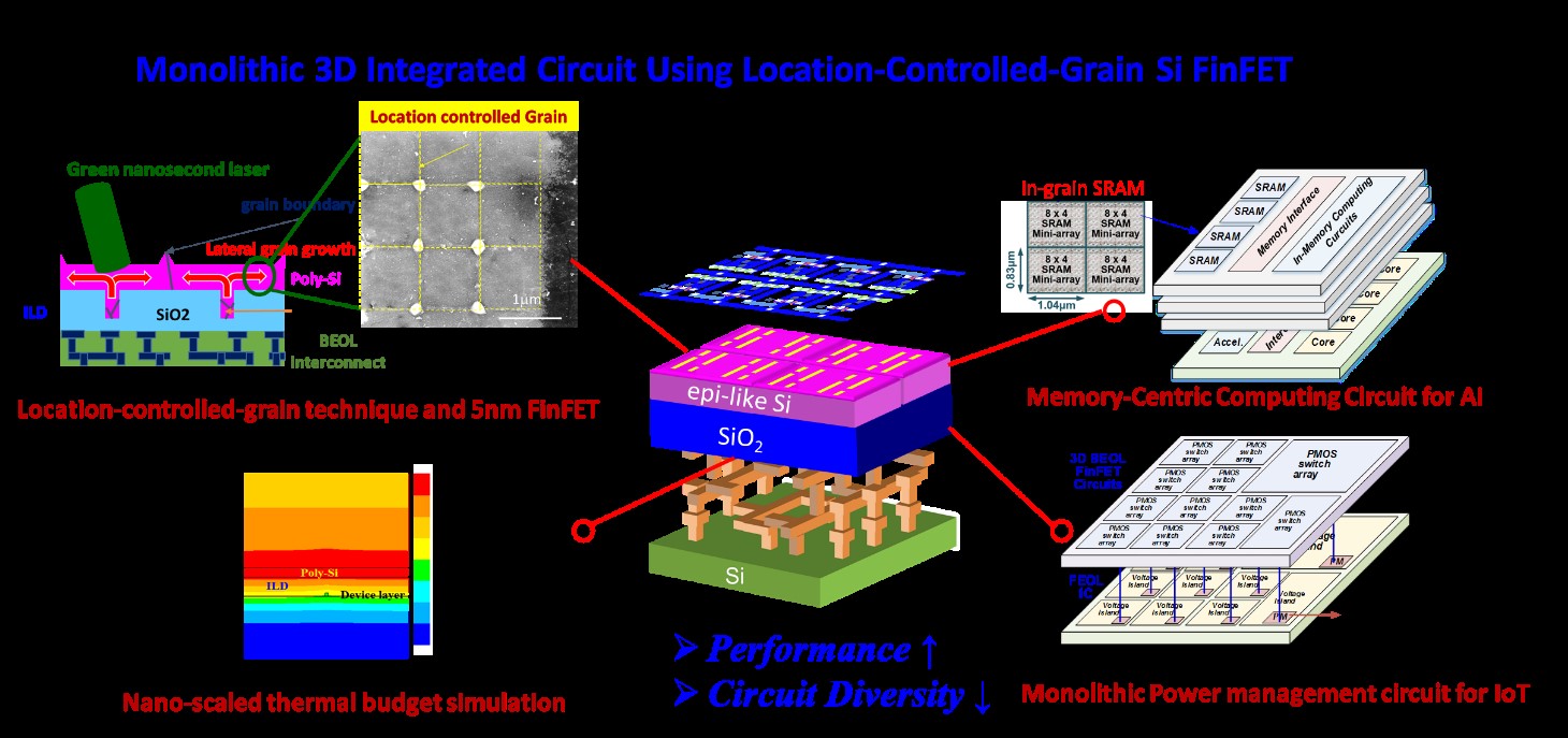
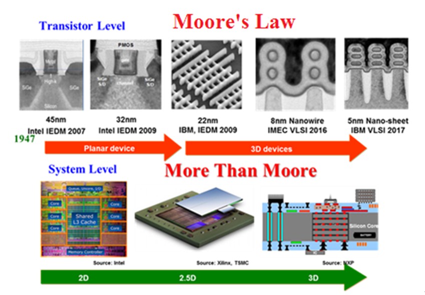
Fig. 1 Moore’s Law & More than Moore
The concept of “More than Moore” is becoming more important as device scaling is becoming more difficult and expensive. The global semiconductor industry is attempting to add value and extend the functionality of integrated circuits for advanced circuit design, for example, in artificial intelligence (AI) and the Internet of Things (IoT) applications. Monolithic 3D (M3D) integration provides a promising way of accommodating multifunctional devices within a single chip. However, the monolithic stacking is limited because the underlying front-end device and circuit cannot afford the risk of electrical property degradation by thermal shack. The key is how to fabricate high-performance 3D stackable devices using low temperature or thermal budget processes for existing devices or circuits without performance degradation under 400oC.
Several pioneer M3D studies have been published in recent years which have developed low temperature/thermal budget processes. One is a laser recrystallized poly-Si channel for monolithic 3D device fabrication with the benefits of simplicity and low cost. The laser process provides an ultra-shallow heating and recrystallization process (~100-300nm in depth) which prevents damage. The only concern is the electrical property variation caused by defects and grain boundaries in the poly-Si channel for circuit design.
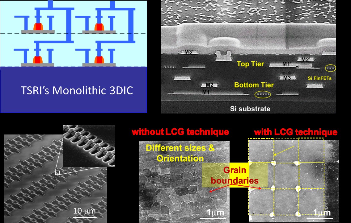
Fig. 2 TSRI’s monolithic 3DIC and FinFETs with and without the location-controlled grain technique
Our monolithic 3DIC research team in Taiwan’s Semiconductor Research Institute (TSRI) aims at manufacturing advanced monolithic 3D devices (e.g., ultra-thin body transistors, nanowire FETs, FinFETs) and related functional units (e.g. SRAM, decoders, etc.) using green nanosecond laser recrystallization, which melts a-Si thin-film into a high-quality poly-Si channel within a short period of time (<1 μs). Recently, we proposed a back-end of line (BEOL) location-controlled-grain (LCG) technique for monolithic 3D integrated circuits in collaboration with the NCTU research team led by Prof. Chenming Hu and Prof. Kuan-Neng Chen. The location of the controlled-grain Si island is determined by a partial “via hole” etched into the interlayer-dielectric, and the grain size is determined by the distance between “vias” due to lateral grain growth. Instead of the random grain growth poly-Si channel without the partial “via etch,” we obtained a regularly patterned array of single-grain Si matrix, which allows the fabrication of FinFETs and circuit units without grain boundaries. It shall dramatically improve the semiconductor chip performance and production yield. In addition, we also collaborated with the NTHU research team led by Prof. Meng-Fan Chang to build up monolithic 3D computing in memory (CIM) units for AI and IoT applications. Over 20 articles (2012-2019) have been published in IEDM and VLSI, which are the world's preeminent forums for reporting technological breakthroughs in the areas of semiconductor and electronic device technology, design, and manufacturing.
Our monolithic 3D integration technology provides efficient connectivity of functional circuits, decreases power consumption, enhances system performance and minimizes chip size for AI and IoT applications. The M3D research service platform welcomes collaboration with the industrial, academic and research sectors in Taiwan. We hope the platform can reduce the time cost for technological development and verification, avoid the waste of resources and become the engine catalyzing the semiconductor research of the industrial, academic, and research communities.
RELATED

STAY CONNECTED. SUBSCRIBE TO OUR NEWSLETTER.
Add your information below to receive daily updates.