From telecom network manager to guardian in digital world – An example of network management transformation

Author(s)
Tung-Ying HsiehBiography
Tung-Ying Hsieh is an Assistant Researcher at NARLabs. He received his Master’s degree in material science and engineering from NTHU. Currently, he is a PhD candidate at the Institute of Electronics Engineering, NTHU. Before he joined NARLabs, he worked at TSMC and TSRI. He has published more than 25 journal articles and has 4 patents in the 3DIC field.
Academy/University/Organization
Taiwan Semiconductor Research Institute-
TAGS
-
Share this article
You are free to share this article under the Attribution 4.0 International license
- ENGINEERING & TECHNOLOGIES
- Text & Image
- April 15,2021
With the advent of the Post-Moore Era, development trends in semiconductor manufacturing have shifted from transistor scaling to a conceptual, innovative challenge. Semiconductors have gradually flourished from a laboratory experiment to a real-world product, eventually even developing into a complex and extremely competitive industry. The Taiwan Semiconductor Research Institute (TSRI) plays an extremely important role in Taiwan's academic and industrial innovation development. This article illustrates the roles and significant achievements of TSRI, and the impact of 3DIC.
Challenges in the post-moore era
As one of the eight laboratories of NARLabs, (a research institute) funded by the MOST, TSRI not only cultivates talented people, but also builds a bridge between industry and academia. In the Post-Moore Era, new technologies such as artificial intelligence, quantum computers, next-generation memory, high-speed computers, 5G, and other emerging applications have all rapidly arisen. As such, we are facing strong challenges from Europe, America, Japan, and South Korea. In order to support Taiwan’s academic and industrial innovation development in this regard, TSRI is entrusted with the following missions:
- To establish semiconductor R&D platforms.
- To support domestic academic research.
- To promote Å (Angstrom) science and technology.
- To foster talented people for practices in high-tech industries.

Fig.1 The “three-dimensional integrated circuit (3DIC)" is in concept like building skyscrapers in a densely populated city, and has become a promising solution to conquer physical limitations. (Image source: Pixabay)

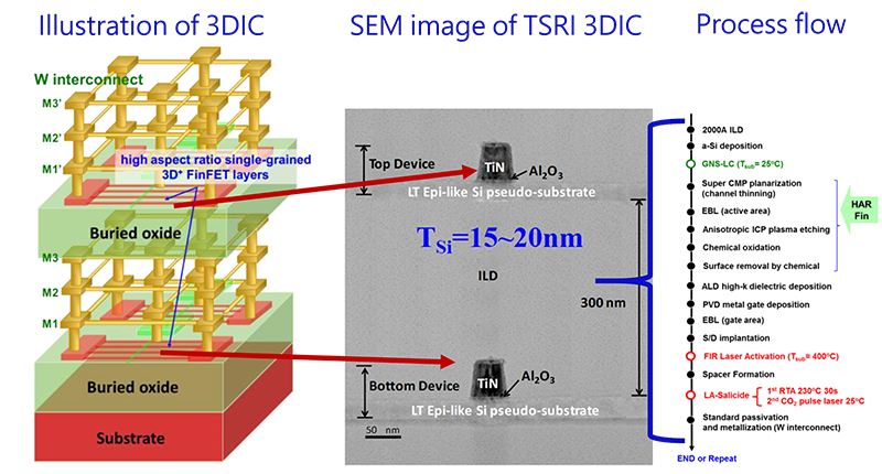
Fig.2 TSRI’s key technologies for 3DIC manufacturing, including the "nanosecond green laser for localized activation" and the "ultra-fast heating method to recrystallize amorphous silicon thin films."
Highlights and achievements in 3DIC research
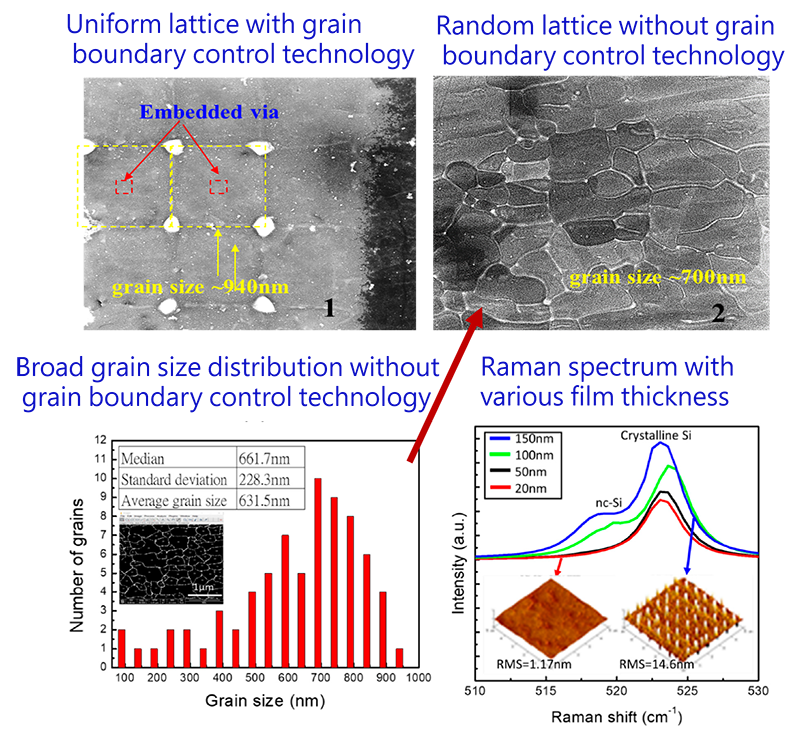
Recent important achievements in 3DIC research include the "nanosecond green laser for localized activation" and the "ultra-fast heating method to recrystallize amorphous silicon thin films." These technologies can be introduced in ultra-thin body (UTB) transistors, nanowire transistors, FinFET and stackable integrated circuits (such as SRAM, Decoders, etc.). According to a report published by the Science & Technology Policy Research and Information Center (STPI), the impact of academic publications and the number of citations can be increased through international cooperation. Therefore, the TSRI attaches great importance to broadening its network and linkage to top international organizations. In recent years, it worked with UC Berkeley to present "grain boundary control technology," and collaborated with National Tsing Hua University to produce computing-in-memory units. Both technologies are for high-performance and power-saving 3DIC application. Related research results have been published in IEDM (International Electron Devices Meeting) and VLSI (Symposia on VLSI Technology and Circuits).

Fig.3 TSRI worked with UC Berkeley to present "grain boundary control technology," which shows a significant improvement in channel quality.
Future application of 3DIC
According to the analysis of industry development trends undertaken by the Industrial Technology Research Institute (ITRI), 3DIC packaging will account for 42.5% of the overall packaging revenue in 2025. From a technological perspective, the concept of three-dimensional integrated circuits can be realized and performed in different approaches, including system-on-integrated-chips (SoIC), integrated fan-out packaging technology InFO (Integrated Fan-out), CoWoS (Chip on Wafer on Substrate) and Monolithic 3DIC. From the application perspective, flat panel displays, self-driving cars, 5G chips, smart phones, and medical display instruments will all benefit from future three-dimensional integrated circuits. As many key technologies of 3DIC are held by Taiwan’s semiconductor manufacturers, global IT industry giants such as Google, Apple, AMDs, and Tesla have all increased their investment in Taiwan.
STAY CONNECTED. SUBSCRIBE TO OUR NEWSLETTER.
Add your information below to receive daily updates.


