

A Breakthrough in the Quantum Circuit Design of Shor's Algorithm
Author(s)
Chee-Wee LiuBiography
Chee Wee Liu's research includes SiGe/GeSn epi/photonics, stacked 3D transistors, thermal simulation (physics-based and neural network-based), IGZO TFT, and solar cells. He demonstrates the record high 2,400,000 ((cm)^2)/Vs electron mobility in strained Si, the first Si cap on SiGe channel, CVD GeSn outperforming MBE in terms of hole mobility, stacked GeSn(p)/GeSi(n) channels, and the first Si/SiGe/SiC MIS LEDs. He also invented the tree transistors beyond FinFET and Stacked GAA.
Academy/University/Organization
National Taiwan University-
TAGS
-
Share this article
You are free to share this article under the Attribution 4.0 International license
- ENGINEERING & TECHNOLOGIES
- Text & Image
- April 22,2020
Autonomous driving is a killer application of AI. Level 5 (mind off) allows autonomous vehicles to perform all driving tasks without human manipulation or attention. To achieve Level 5, high performance and low power ICs are needed to tackle real-time computational loads and guarantee safety and reliability. Thus, transistors play an important role in achieving this target. Professor Liu’s group is dedicated to research on high performance and low power transistors.
Gate-all-around (GAA) is considered a promising architecture for superior electrostatics control of the channel to achieve low power consumption, and extends the scaling beyond FinFET limits. The vertically stacked GAAFETs can further provide a large drive current for a given footprint to achieve high performance and area scaling in the advanced technology nodes. Ge is a good channel material owing to its intrinsic higher electron and hole mobility as compared to Si which is considered as one option to further enhance the performance. We thus demonstrated vertically stacked tensily strained Ge0.98Si0.02 nGAAFETs in 2019 IEDM.
In the as-grown epi-layer, an additional 800oC annealing after the Ge buffer growth on silicon on insulator (SOI) further improves the epi-layer quality by confining misfit dislocations near the Ge buffer/Si interface. The stacked Ge0.98Si0.02/Ge layers were grown on the Ge buffer at a low temperature of 350oC. Due to the thermal expansion coefficient mismatch between Ge and Si, the Ge buffer is 0.12% tensily strained after the 800oC annealing, and the Ge0.98Si0.02 layers have 0.2% tensile strain. The Ge0.98Si0.02 channels with only 2% Si can ensure the electrons in L valleys and introduce minimal alloy scattering. The unintentionally doped channels can reduce impurity scattering, and heavily doped ([P]~2.7E20 cm-3) Ge sacrificial layers can reduce Source/Drain parasitic resistance. The good photoluminescence of the epi-layer indicates sufficiently low point defect density.
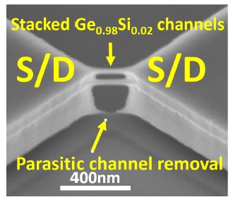
For channel release, ultrasonic-assist TMAH etching at 60oC was used to completely remove the Si underneath the Ge buffer. Finally, the Ge buffer and the Ge sacrificial layers in the channel region were completely etched by optimized ultrasonic-assist H2O2 to form the two stacked Ge0.98Si0.02 nanowires without a parasitic channel. After the channel release process, the uniaxial tensile strain in the channel is further enhanced to 0.27%. Ge0.98Si0.02 has 1.3X the mobility of relaxed Ge by estimation.
The device with the 500oC post metal annealing (PMA) process results in a negative threshold voltage (VT) shift as compared to no PMA device. VT is tuned towards zero to have an advantage in low power applications. The gate length (LG) of the device is scaled to 40 nm by further optimizing the ebeam patterning. Devices with 500oC PMA, a large cross section, and scaled LG = 40 nm reach ION = 48 µA (3.2X improvement) at VOV = VDS = 0.5 V as compared to devices with the same 500oC PMA, a small cross section, and LG = 60 nm. Gm,max reaches 136 µS (3.4X improvement) at VDS = 0.5 V. Devices with a large cross section need more negative VGS than those with a small cross section to completely deplete the channel. Devices with 500oC PMA, a large cross section, and scaled LG = 40 nm have the highest ION per stack among Ge nFETs, and are comparable to Si nFETs. Record Gm,max(µS/µm)/SSSAT(mV/dec) of 8.3 is achieved among Ge nFETs.
Therefore, an optical non-destructive method is developed to check the existence of parasitic channels underneath the stacked Ge0.98Si0.02. Under the 1310 nm infrared illumination, devices without a parasitic channel have a negative VT shift, while devices with the Ge parasitic channel have a photocurrent. The photoresponse method is consistent with SEM micrograph and provides a non-destructive method to check the existence of parasitic channels.
Excellent electrical characteristics are achieved with record ION and record Gm,max(µS/µm)/SSSAT(mV/dec) among Ge nFET. High [Ge] of 98% in GeSi with L valley conduction and 0.27% tensile strain in the channels from the microbridge structure are also helpful for high ION. The performance of our Ge0.98Si0.02 channels is comparable to that of Si channels.
RELATED


STAY CONNECTED. SUBSCRIBE TO OUR NEWSLETTER.
Add your information below to receive daily updates.