

The recent development of high-performance organic photovoltaics

Reference: http://tecofound.org.tw/teco-award/2020/download/prev-winner_27_01.pdf
Author(s)
Edward Yi ChangBiography
Prof. Edward Yi Chang received his PhD degree in Materials Science and Engineering at the University of Minnesota, USA. Prof. Edward is a Senior Vice President and Dean of the International College of Semiconductor Technology, NYCU. He is also the Director of the NCTU-TSMC Research Center. Prof. Edward was awarded IEEE Life Fellow, JSAP Fellow by the Japanese Applied Physics Society and Taiwanese Materials Society Fellow.
Academy/University/Organization
National Yang Ming Chiao Tung UniversitySource
CSD Lab-
TAGS
-
Share this article
You are free to share this article under the Attribution 4.0 International license
- ENGINEERING & TECHNOLOGIES
- Text & Image
- April 14,2021
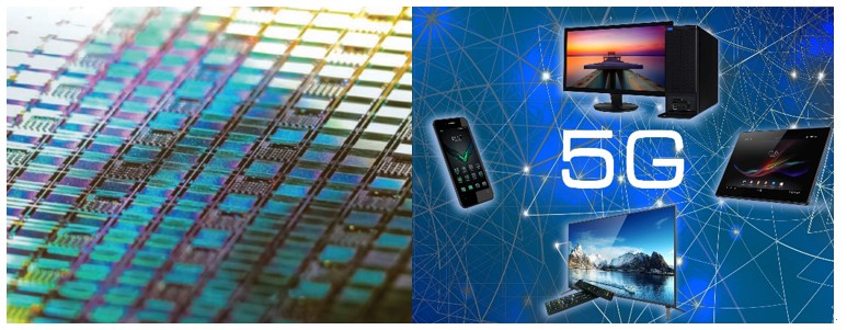
III-V semiconductor materials have excellent material properties which offer a great deal of freedom to develop state-of-the-art high frequency devices for advanced 5G communication, cutting-edge power, and low power logic applications. The Compound Semiconductor Lab (CSD Lab) is led by Prof. Edward Yi Chang, who has always been dedicated to building cutting-edge device technologies with high quality III-V epitaxial heterostructures and devices. In recent years, Prof. Chang and his team have successfully developed an InGaAs-based Quantum Well Field Effect Transistor (QWFET) with a world-record cut-off frequency of 750GHz, and have also developed an AlGaSb epitaxy material on a silicon substrate with a world-record electron mobility of 27300 cm2/ (V·s). To meet the needs for 5G communication, the team has developed a GaN high frequency power device with a power density of 10W at Ka Band. Also, his team is expanding research on GaN devices for high operating frequency and high output power density power electronics, which is very suitable for millimeter wave, terahertz, advanced radar communications, electrical vehicles, wireless chargers and medical imaging applications.
The future of "III-V compound semiconductors"
Heterogeneous materials integration, advanced process technology and chip-level integration are the major challenging domains for the next generation of semiconductor technology. III-V compound semiconductor materials are recognized as promising candidates for high frequency and high power electronics applications for the past 3 decades. III-V compound semiconductors have superior electronic properties, which are highly suitable for cutting-edge advanced 5G communication systems, SATCOM (millimeter wave) and radar communication systems, low and high power electronics for electrical vehicles, wireless chargers, and solar cell applications.
Lab overview – "Materials to chip-level packaging"
With 20 years of semiconductor industrial experience, Prof. Edward Yi Chang established a Compound Semiconductor Device Lab (CSD Lab, NCTU) to address the technological breakthroughs in GaAs, InP and GaN based High Electron Mobility Transistors (HEMT) and Heterojunction Bipolar Transistors (HBT), InGaAs FinFET for RF and low power logic application with the support of the Ministry of Science and Technology (MOST), Taiwan. Prof. Chang realized that combining dissimilar materials (III-V) using metal organic chemical vapor deposition (MOCVD) and processing with a multi-step sequence will ultimately strengthen the device integrity. He and his team have established a MOCVD epitaxial system for larger wafer size and advanced processing units for GaN high power, high frequency devices, GaAs/Ge/Si heterostructure for solar cell applications and InGaAs/Si for Radio Frequency (RF) and low power logic applications. The CSD Lab is continuously updated with advanced cutting-edge technology node processing tools, such as e-beam lithography for < 50 nm technology nodes, Atomic layer deposition for High-K dielectric, e-gun metal deposition for ohmic and gate metal, ICP etching, and plasma-enhanced chemical vapor deposition. In addition, the CSD lab supports flip-chip package technology in order to enhance the GaN HEMT system performance for high speed and high frequencies.
Achievements
Over the years, Prof. Chang and his team have achieved world-record device performances in international academia and in science parks in Taiwan. The CSD Lab is the only university lab that provides 4-inch III-V device pilot line service with capability down to 60nm, which gives the lab an advantage in a field of such competence.
In recent years, Prof. Chang and his team have set a new world record by developing the world's highest frequency ft to 750 GHz from a novel InAs-based Quantum Well Field Effect Transistor (QWFET) which is suitable for submillimeter-wave applications. Also, the CSD Lab has succeeded in making AlGaSb-based transistors with a record-high electron mobility of 27300 cm2/ (V·s). To further meet the RF and power requirements of weapon detection for national security purposes, the CSD Lab has developed GaN high electron mobility transistors (HEMTs) with power density of 10 W/mm measured in a Ka Band environment. Meanwhile, a complete pilot line for AlGaN/GaN and GaAs devices, Prof. Chang and his team aim to integrate the epitaxial growth of III-V semiconductor heterostructures and high frequency device process technology to make it compatible with CMOS production lines and ready for high yield mass production.
Prof. Chang has produced more than 500 technical papers in reputed international journal and conference proceedings, and holds four patents. He won several "Outstanding Contributions Awards for Cooperation of Industry and Academia" and “Outstanding Research Awards" over 22 years of academic experience.
Industrial and Academic partners
In order to transfer the knowledge of the CSD lab and its innovation, Prof. Chang has been building cooperative relationships with world leading semiconductor industries, such as TSMC, Intel Corp., WIN semiconductors, imec, MIT, Panasonic Corp., Sharp Lab, Malaysia Telecom, Samsung Cheil Corp., and Veeco. The leading epitaxy and processing technologies developed by the CSD Lab have contributed royalties of more than 130 million NT dollars, which indicates its industrial competitiveness and value.
Prof. Chang has been very active in cooperating with international leading institutes, the cooperation partners include labs from UC Berkeley (USA), Penn State University (USA), Virginia Tech (USA), MIT (USA), ATMI (USA), TIT (Japan), NTT (Japan), IMEC (Belgium), Chalmers University (Sweden), Queens University (UK) and Hong Kong University of Science and Technology (China). The results have been disseminated in the form of high quality publications. The important findings from these collaborations have resulted in successful technology transfer, which acts as another driving force for developing advanced III-V semiconductor devices in the 5G era. Prof. Chang strongly encourages doctoral students to enroll and carry out their research across different universities worldwide for valuable international experience.
The CSD Lab looks forward to continued co-operation with pioneering semiconductor industries and top universities around the world when the III-V semiconductor will keep shining in the darkest nights.
RELATED
STAY CONNECTED. SUBSCRIBE TO OUR NEWSLETTER.
Add your information below to receive daily updates.