Taiwan and Sri Lanka Environmental Change Sciences and Technology Innovation Center- a Preliminary Survey of Nutrient and Car...

Author(s)
Yu-Jung LuBiography
Dr. Yu-Jung Lu is an Assistant Research Fellow of the Research Center for Applied Sciences at Academia Sinica and an Assistant Professor of the Department of Physics at National Taiwan University. Dr. Lu received her Ph.D. in Physics from National Tsing Hua University in 2013. She worked at California Institute of Technology (Caltech) as a postdoc from 2015 to 2017. She is a material physicist, and her research interests are within an interdisciplinary field of active plasmonics/optoelectronics with a particular focus on semiconductor nanostructure devices to investigate harvesting, generating, and manipulating light at the nanoscale.
Academy/University/Organization
National Taiwan UniversitySource
https://pubs.acs.org/doi/10.1021/acsnano.0c04224-
TAGS
-
Share this article
You are free to share this article under the Attribution 4.0 International license
- NATURAL SCIENCES
- Text & Image
- December 21,2020
To date, the size of conventional lasers is usually larger than half the wavelength due to the diffraction limit, which hinders their applications in on-chip integration and ultracompact optoelectronic devices. The miniaturization of optoelectronic components has gradually become an important research topic, especially for nanolasers. How can the size of the laser be reduced? How can the energy consumption of the laser operation be reduced? How can a laser with a new working mechanism be developed to overcome the diffraction limit? These have become the key challenges for nanolasers.
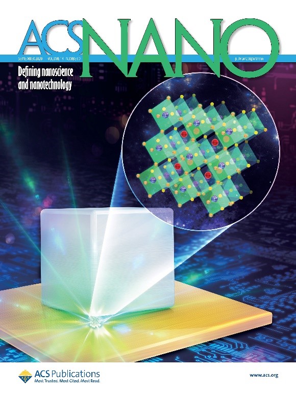
Recently, Prof. Yu-Jung Lu, an Assistant Research Fellow at Academia Sinica, and her collaborative research teams have published on continuous-wave nanolasing from a single lead halide perovskite (CsPbBr3) quantum dot in a plasmonic gap-mode nanocavity with an ultralow threshold. This work was published in ACS Nano as the selected cover issue. This is the first continuous wave operation of a lead trihalide perovskite nanolaser with a record low lasing threshold of 1.9 W cm-2 at 120 K, and it has a temporal coherence feature for measuring the second-order correlation function; more significantly, it sets a state-of-the-art record for the ultrasmall mode volume (~0.002 λ3), which is much smaller than the diffraction limit. This work is the first known example of lasing from a single quantum dot integrated with a plasmonic nanocavity. The ultrasmall mode volume of the nanolaser leads to desirable device properties, such as low power consumption and fast switching, which will benefit its application in future ultracompact integrated circuits for optical communication and quantum information processing.
To date, the size of conventional lasers is usually larger than half the wavelength due to the diffraction limit, which hinders their applications in on-chip integration and ultracompact optoelectronic devices. The miniaturization of optoelectronic components has gradually become an important research topic, especially for nanolasers. How can the size of the laser be reduced? How can the energy consumption of the laser operation be reduced? How can a laser with a new working mechanism be developed to overcome the diffraction limit? These have become the key challenges for nanolasers.
Recently, Prof. Yu-Jung Lu, an Assistant Research Fellow of the Research Center for Applied Sciences at Academia Sinica, and her collaborative research teams have published on continuous-wave nanolasing from a single lead halide perovskite (CsPbBr3) quantum dot in a plasmonic gap-mode nanocavity with an ultralow threshold. This provides an approach for realizing on-chip electrically driven lasing and integration into plasmonic circuitry for information processing. This work was published in ACS Nano as the selected cover issue this year.

Ultralow-threshold Plasmonic Nanolaser by Using a Single Perovskite Quantum Dot
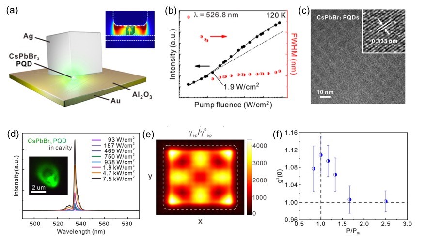
The nanocavity is designed as a sandwich structure in which a single highly emissive perovskite quantum dot is located between a silver nanocube and a gold substrate, as shown in Figure 2a. A thin layer of Al2O3 was deposited between the perovskite quantum dot and the gold substrate to avoid PL quenching. This is the first continuous wave operation of a lead trihalide perovskite nanolaser with a record low lasing threshold of 1.9 W cm-2 at 120 K (see Figure 2b), and it has a temporal coherence feature for measuring the second-order correlation function (see Figure 2f). More significantly, it sets a state-of-the-art record for the ultrasmall localized mode volume (~0.002 λ3), which is at least two orders of magnitude smaller than the optical diffraction limit.

Lasing characteristics and the lasing mechanism of a single perovskite quantum dot (PQD) in a localized gap plasmon cavity at 120 K. Besides, the temporal coherence signature of the PQD nanolasing under 120 K was determined.
The other key reason for this success is the development of lead trihalide perovskite quantum dots, which were prepared by a novel spray synthesis method that has extraordinary optical properties. A transmission electron microscopy image of the synthesized CsPbBr3 perovskite quantum dots is shown in Figure 2c. The average size of the quantum dots is approximately 10 nm, and the high crystallinity feature is confirmed. Note that a semiconductor with high crystallinity may eliminate the nonradiative recombination pathways and enhance the emission. Thus, the features of high quantum yield and high optical gain coefficient make the device easily achieve lasing. The first author, Yu-Hung Hsieh is a Ph.D. student in National Tsing-Hua University, who theoretically shows that the localized Purcell enhancement and the coupling strength for the single quantum emitter can be tailored by varying the dipole orientation and the position of the quantum dot (see Figure 2a and 2e). Under particular conditions, lasing can be achieved. This is the reason why only approximately 30% of the measured devices show lasing features.
In addition, the authors have carried out detailed theoretical simulations that shed new light on the understanding of the novel lasing mechanism in gap-mode plasmonic nanolasers. This work is the first known example of lasing from a single quantum dot integrated with a plasmonic nanocavity. The ultrasmall mode volume of the nanolaser leads to desirable device properties, such as low power consumption and fast switching, which will benefit its application in future ultracompact integrated circuits for optical communication and quantum information processing. More recently, Prof. Lu’s research team has continued to work on the perovskite-based upconversion plasmonic nanolasers, electrically driven nanolasers, and room-temperature enabled plasmonic nanolasers with low threshold (low power consumption).
More information: Y-H Hsieh et al., Perovskite Quantum Dot Lasing in a Gap-Plasmon Nanocavity with Ultralow Threshold, ACS Nano 14, 11670–11676 (2020).
STAY CONNECTED. SUBSCRIBE TO OUR NEWSLETTER.
Add your information below to receive daily updates.


