

Semantic Segmentation on UAV Images for large-scale Agriculture Damage Assessment

Ultraviolet Plasmons empowered photodetector of ultrahigh responsivity, detectivity, and broad bandwidth using single-crystalline Aluminum nanoholes array
Author(s)
Ta-Jen YenBiography
Prof. Ta-Jen YEN received his Ph.D. from Mechanical and Aerospace Engineering, UCLA. Dr. YEN joined Department/Institute of Materials Science and Engineering (MSE), National Tsing Hua University (NTHU) in 2005, and then served as a director of the Division of Student Activities, a director of the Division of Intellectual Property and Technology Licensing, and a Chair of the MSE. Currently Prof. YEN is a Vice President of Global Affairs and meanwhile the youngest director of Material Research Society and executive director of TISA in Taiwan. Recently Prof. YEN received several awards, such as Excellent young scholar from CoE and NTHU, Excellent Young Scholar projects from ministry of Science and Technology (MOST), Taiwan, in a row, Excellent Teaching Award of CoE and NTHU (2009), and Excellent Teaching Award of Engineering College at NTHU (2012), Ta-You Wu Memorial Award of MOST, Taiwan. Currently, Prof. YEN research focuses on metamaterials, Plasmonics, nanodevices, biomedical photoelectrical detection and so on.
Academy/University/Organization
National Tsing Hua UniversitySource
https://onlinelibrary.wiley.com/doi/full/10.1002/advs.202002274-
TAGS
-
Share this article
You are free to share this article under the Attribution 4.0 International license
- ENGINEERING & TECHNOLOGIES
- Text & Image
- December 21,2020
For many years, photodetectors have been fabricated using several wide band gap semiconductors. To enrich the performance of these photodetectors, several techniques have been investigated. Visible and IR regime plasmonics are among them. However, ultraviolet (UV) plasmonics remain unavailable mainly because of a lack of suitable materials. So far, the most used materials for plasmonic photodetectors are silver (Ag) and gold (Au). Therefore, in this work, we empower superior photodetection using single-crystalline Al film on wide band-gap semiconductor gallium nitride (GaN). By fabricating a periodic nanoholes array on this single-crystalline Al film, we enable localized surface plasmon resonance (LSPR) and extraordinary transmission, and thus demonstrate the maximum responsivity and highest detectivity at the resonance wavelength of 355 nm. Finally, a Schottky contact forms between the single-crystalline Al and GaN substrate, leading to the fast temporal response of a rise time and a fall time. Based on our knowledge, the presented detectivity is the highest compared with the other reported GaN UV photodetectors.
For UV photodetection, a wide bandgap semiconductor like GaN is a prominent candidate because it has a large absorption coefficient in the UV spectrum along with chemical and thermal stability. Thus, GaN designed photodetectors based on metal-semiconductor-metal (MSM), p-i-n, p-n, Schottky, and avalanche junction have been portrayed form a long interval. Among them, Schottky photodetector has been triggered due to no p-type doping, low dark current, high responsivity, and detectivity. For GaN-based UV Schottky photodetectors, numerous significant approaches have been used to escalate the absorption, responsivity and quantum efficiency [1].
In this work, our research group realizes an innovative measure of Al plasmonics on conventional GaN, demonstrating an ultrasensitive UV photodetector with the greatest detectivity compared with other reported GaN photodetectors [2]. Al is the most vital and abundant metal and shows further advantages of high plasma frequency (~15 eV) and low screening (ε∞ ~ 1), but in fact, it is controversial to adopt Al for plasmonic applications because its great intrinsic loss dramatically damps the resonance strength. To reduce the intrinsic loss from grain boundaries and internal defects, herein we employed the method of plasma-assisted molecular beam epitaxy, to fabricate a single-crystalline Al film. Not only does this single-crystalline Al film possess lower intrinsic loss, but also form a Schottky contact with the GaN substrate to intensify the photocurrent generation.
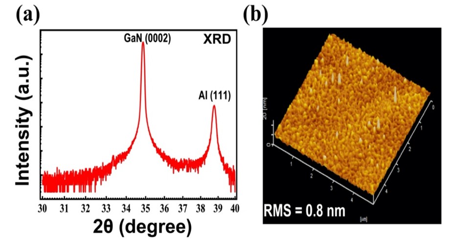
Figure 1. (a) X-ray diffraction (XRD) measurement of single-crystalline Al film on GaN/Al2O3 shows the XRD peak of GaN (0002) and Al (111) peak at 34.8˚ and 38.7˚ respectively. (b) Atomic force microscopy (AFM) image (area: 5 µm x 5 µm ) shows surface roughness of epitaxial single crystalline aluminum film on GaN substrate.
In plasma-assisted molecular beam epitaxial process, we monitored the in-situ growth of single-crystalline Al films by using streaky reflection high-energy electron diffraction patterns. Then, we observed ex-situ characterization of the excellent crystallinity of the atomically epitaxial and smooth film, as shown in Figure 1.
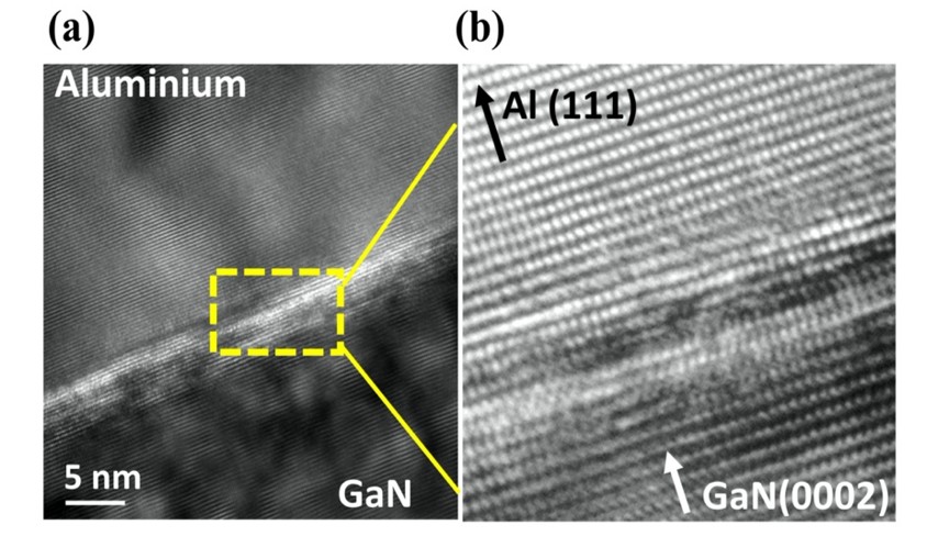
Figure 2. (a) and (b) Interface Transmission electron microscope (TEM) image shows atomic arrangement of single crystalline Al (111) film on GaN (0002) substrate.
The fabricated Al film is certainly with the outstanding quality, but how can we excite plasmons and make the incident UV light propagating through it to reach GaN to produce photocarriers? To answer this question, we introduced a periodic nanohole array in the epitaxial Al film (see Figure 3(a) and (b), respectively). Such a periodic nanohole array supports the excitation of localized surface plasmon resonance modes, leading to extraordinary transmission (EOT) [3], as shown in Figure 4(a). For this periodic nanohole array, we optimized its periodicity and diameter, respectively, to achieve ultrahigh responsivity, detectivity, and broad bandwidth. First, with the optimized periodicity of 320 nm, we achieved a maximum EOT at the GaN surface at 355 nm resonant wavelength. As incident light matching plasmonic resonance wavelength, the device shows exceptional photodetection performance.
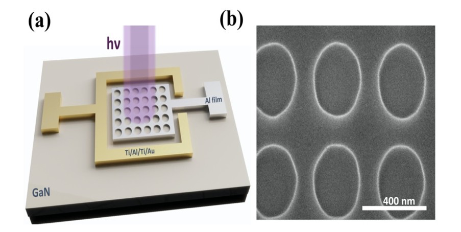
Figure 3. (a) Schematic design of Al enriched UV Photodetector (b) Scanning electron microscopy (SEM) image of periodic Al nanohole array with 220 nm diameter and 320 nm periodicity
For example, we observed the maximum responsivity of 670 A/W at an 11 nW illumination and the maximum detectivity of 1.48 × 1015 cm Hz1/2 W-1, as shown in Figure 4(b). The UV photodetection demonstrated here presents the highest detectivity among the reported GaN photodetectors [2]. In addition, with the optimized diameter of 220 nm, we not only excited higher resonance modes, but also activated plasmonic coupling among nanoholes to broaden the spectral photo enhancement. As a result, the bandwidth of this deliberately designed photodetector appeared very broad, encompassing the entire UV range from deep UV to near UV spectra. Evidently, our UV photodetector also outperformed others for 325 nm and 266 nm incident wavelengths, as shown in Figure 4(c).
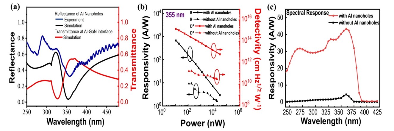
Figure 4. (a) Experimental/simulation reflectance measurement of Al nanohole array measured and simulated (FDTD) transmittance at Al and GaN interface (red curve) to show EOT phenomena (b) Calculated Responsivity (R) and detectivity (D*) as function of 355 nm laser illuminated power. (c) Spectral responsivity spectra of as fabricated photodetector with and without Al nanohole array from deep UV to near UV regime.
Finally, as illustrated in Figure 5(a), a Schottky contact was formed between the single-crystalline Al nanohole array and the GaN substrate. As the excited plasmons decay in to charge carriers, these hot electrons rapidly transferred in to GaN and drive through the other electrode, resulting in a fast temporal response with a rise time of 51 ms and a fall time of 197 ms, as presented in Figure 5(b). In addition, the exponential decay behavior of photocurrent and large difference in rising and falling time is attributed to the persistent photoconductive behavior of GaN. In summary, based on the aforementioned merits of ultrahigh responsivity, detectivity, broad bandwidth, fast temporal response and CMOS compatibility, we believe that this Al plasmonics enriched UV photodetector paves a route towards practical applications in defense, UV astronomy, biological, and medical sciences and others [4].
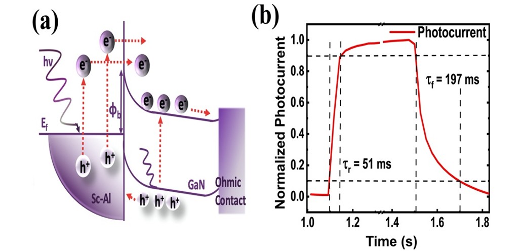
Figure 5. (a) schematic energy band alignment of photodetector at reverse bias. (b) Calculation of rising and falling time of photodetector for 355 nm laser excitation. 51 ms and 197 ms.
References :
- H. Chen, K. Liu, L. Hu, A. A. Al-Ghamdi, X. Fang, Mater. Today 2015, 18, 493.
- L. Liu, C. Yang, A. Patanè, Z. Yu, F. Yan, K. Wang, H. Lu, J. Li, L. Zhao, Nanoscale 2017, 9, 8142.
- T. W. Ebbesen, H. J. Lezec, H. F. Ghaemi, T. Thio, P. A. Wolff, Nature 1998, 391, 667.
- W. Ouyang, F. Teng, J.-H. He, X. Fang, Adv. Funct. Mater. 2019, 29, 1807672.
RELATED


STAY CONNECTED. SUBSCRIBE TO OUR NEWSLETTER.
Add your information below to receive daily updates.