

Are You Ready for Industry 3.5?
Author(s)
Yuan-Chieh TsengBiography
Prof. Yuan-Chieh Tseng is a distinguished professor of NCTU. He is also the Associate Vice President of the Office of International Affairs. He is an expert in spintronics/magnetism, participating in organizing many international conferences in magnetism. He was the chair of the User Executive Committee, National Synchrotron Radiation Research Center (NSRRC), 2016.
Academy/University/Organization
National Chiao Tung UniversitySource
https://pubs.acs.org/doi/10.1021/acsami.9b11767-
TAGS
-
Share this article
You are free to share this article under the Attribution 4.0 International license
- ENGINEERING & TECHNOLOGIES
- Text & Image
- April 21,2020
Complementary metal-oxide-semiconductor (CMOS) technology has been the workhorse of the semiconductor industry since the 1980s. With the increasing importance of mobile devices, there is high demand for beyond-CMOS technology with high scalability and low power consumption. Magnetoelectric spin–orbit (MESO) devices are believed to be that kind of technology. MESO comprises two technologically scalable transduction mechanisms: magnetoelectric switching and topological conversion of spin to charge. Our team is committed to developing critical materials related to these two transduction mechanisms. We synthesized a new magnetoelectric perovskite of ferroelectric and canted antiferromagnetic orders at room temperature. We found that this compound enables voltage-controlled magnetism when connected with a ferromagnetic layer, in which the device’s magnetic order can be controlled very effectively within a low voltage regime (+/-1 volt). Independently, we investigated the spin-orbit energy of topological insulators and the field-free spin-orbit switching of ferromagnet/heavy-metal heterostructures. The ultimate goal of our research is to combine these two transduction components to form a MESO logic with low-voltage (<1 volt) scalable interconnects, and we have demonstrated its non-volatility and superior switching energy in comparison with CMOS.
The scaling of transistor technology was made possible by controlling the conductivity of semiconductors through the application of an electric field across an insulating gate dielectric. This fundamental principle has remained largely unchanged since the 1980s. Despite the considerable advances in scaling the size of transistors, voltage and frequency scaling has been slow. Efforts to decrease operating voltages have been hampered by the ‘Boltzmann tyranny’ pertaining to electric current control (limit of ln(10) kT/q or 60 mV/dec of electric current at room temperature). This has prompted considerable research efforts to develop beyond-CMOS devices. However, researchers have yet to devise a technologically suitable computational logic device with high energy efficiency, high logic density (i.e., computing functions per unit area), non-volatility (to counteract current leakage) and efficient interconnects.
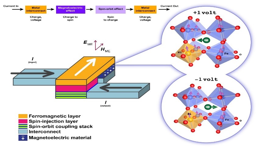
In 2019, the magnetoelectric spin–orbit (MESO) device was proposed. It comprises two technologically scalable transduction mechanisms: ferroelectric/magnetoelectric switching and topological conversion of spin to charge. The device interfaces with electrical interconnects (i.e., it is charge-/voltage-driven) and produces a charge/voltage output, as shown in the representative figure above. The MESO device comprises a magnetoelectric switching capacitor, a ferromagnet, and a spin-to-charge conversion module. Compared to CMOS technology, the MESO device features superior switching energy, lower switching voltage and higher logic density than CMOS. Furthermore, its non-volatility enables the ultralow standby power critical to modern computing.
Our research group is committed to developing materials for the continued development of these two transduction mechanisms. We recently synthesized a novel magnetoelectric perovskite, GdNixFe1-xO3 (GFNO), via sputtering on a SrTiO3 substrate. The proposed GFNO comprises ferroelectric (FE) and canted antiferromagnetic (AFM) orders within a monoclinic framework at room temperature. It exhibits a FE polarization of 37 μC/cm2. When capped with a layer of Co, the resulting heterostructure exhibits voltage-controlled magnetism (VCM) with two distinct features. First, the VCM depends on the magnitude as well as the polarity of the applied bias, thereby doubling the number of available magnetic read-out states under a fixed voltage. Second, the magnetic order of the device can be controlled very effectively to within +/-1 volt. These characteristics satisfy the requirements for low-power MESO operations.
In our research on spin-to-charge conversion materials, we have examined topological insulators with a focus on the issue of tunable spin-orbit energy with thickness- and interface-control. We have also developed field-free spin-orbit switching devices based on a ferromagnet-AFM heterostructure. These material systems are classed as spin-orbit coupling (SOC) materials, but are equally important as magnetoelectric materials in MESO devices.
Our objectives of the current research are to integrate magnetoelectric and SOC material systems and to create a scalable beyond-CMOS spintronic logic device featuring non-volatility and energy-efficient charge-based interconnects. We expect that this device will allow (i) continued scaling in energy per operation toward atto-joule-level switching energy, (ii) substantial improvements in logic density, and (iii) improved scalability for interconnects due to reduced susceptibility to the effects of resistivity. It will also be necessary to devise a path capable of seamlessly integrating the new device with existing CMOS technology.
We believe that the non-volatility and ultra-low energy operations of MESO logic devices will open the door to entirely new computing architectures capable of avoiding the trade-offs inherent in the Turing and von Neumann architectures and Amdahl’s law. New quantum materials, novel integration systems, and alternative logic architectures will usher in the next era of computing beyond advanced CMOS technology.
RELATED
STAY CONNECTED. SUBSCRIBE TO OUR NEWSLETTER.
Add your information below to receive daily updates.