

SP-ISAC: The Best Cybersecurity Partner for High-Tech Industries in Science Parks
Author(s)
Ming-Tsang LeeBiography
Dr. Ming-Tsang Lee received his Ph.D. degree from UC Berkeley. In 2018, he joined the Department of Power Mechanical Engineering in National Tsing Hua University (NTHU) as a faculty member. His research field encompasses laser-assisted micro/nanoscale manufacturing and material processing, multiscale heat transfer, and multiphysics transport phenomena.
Academy/University/Organization
National Tsing Hua UniversitySource
https://doi.org/10.1021/am503897r-
TAGS
-
Share this article
You are free to share this article under the Attribution 4.0 International license
- ENGINEERING & TECHNOLOGIES
- Text & Image
- August 20,2020
Wearable and flexible electronics have boosted the need for circuitry on flexible and, in some cases, transparent substrates. However, most flexible substrates are not compatible with conventional micro-fabrication processes of microelectronics because most of these substrates are chemically and thermally sensitive. The mismatch of the thermal and mechanical properties of the substrate and the functional materials also generally leads to poor adhesion. In addition, for fabricating flexible substrates, a roll-to-roll configuration would be favorable for mass production. Thus, we presented a novel laser-assisted micro/nanoscale fabrication technology: Laser direct synthesis and patterning technology (LDSP): A simple and fast method is needed for fabricating patterns of functional materials on flexible substrates at low processing temperatures and normal (non-vacuum) environments, and could be scaled-up for mass production. In the LDSP process, functional materials are synthesized, deposited and patterned in-situ on flexible substrates using laser-induced photo-thermal reduction of ions from the precursor of the target functional material that is free of nanomaterials. This novel microfabrication technology is cost-effective and eco-friendly. A prototyping intelligent LDSP manufacturing system is currently under development. Micro-transport analysis in triple-phases (solid, substrate, reactive liquid and possibly vapor) and mechanics analysis have been carried out to investigate the critical factors of the process. Artificial intelligence in conjunction with machine vision and machine learning are applied to improve the efficiency of the process. By expanding the types of compatible materials and equipped advanced intelligence, the LDSP aims for the next generation of smart and green manufacturing technology for flexible and wearable electronics.
Flexible electronics such as smart devices, touch panels, solar cells, and personal sensors have boosted the need for circuitry on flexible and, in some cases, transparent substrates. However, most flexible substrates are unsuitable for conventional micro-fabrication processes of electronics because most of these substrates are chemically and thermally sensitive. In addition, the mismatch of the thermal and mechanical properties of the substrate and the functional materials to be deposited often leads to poor adhesion, and affects the mechanical durability of the fabricated device. Furthermore, for a flexible substrate, a roll-to-roll manufacturing configuration would be a great advantage. However, it is very difficult to accommodate such a configuration in conventional microfabrication systems. Thus, a simple and fast method is needed for fabricating patterns of functional materials on flexible substrates at low processing temperatures and normal (non-vacuum) environments, and could be scaled-up for mass production.
Here we present a novel laser assisted micro/nanoscale fabrication technology: Laser direct synthesis and patterning (LDSP), which is a promising way to realize flexible electronic circuitry. In a typical process, a thin layer of coated nanomaterials on the substrate is applied as both the laser energy absorber and the seed functional material to promote the material synthesis in the subsequent laser scanning that uses reactive ionic precursors to grow the nanostructures. A representative LDSP process is illustrated schematically in Figure 1. Liquid solution containing ions of the target material used as the precursor is spread on the substrate. A laser beam which can be absorbed by the solution and/or the pre-deposited nano-seeds is focused on the interface between the solution and the substrate and moved by using a galvano-mirror scanner. Nanoparticles and/or nanofilms of the target functional material are produced from chemical reaction confined in the focused laser heated solution, and are immediately sintered and deposited by absorbing laser energy to form microstructures with predetermined patterns.
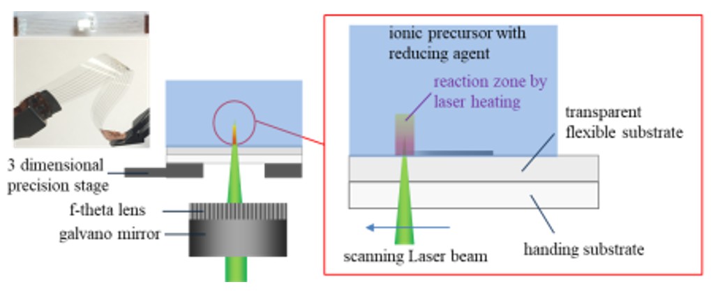
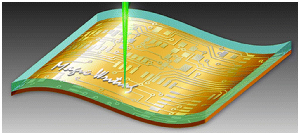
Figure 1. Illustration of the laser direct synthesis and patterning (LDSP) process for functional materials on a transparent and flexible polymer substrate. (courtesy of MT Lee’s group at NTHU)
Figure 2 shows examples of highly conductive micro-patterns on a polyethylene terephthalate film for demonstrating the capability of this LDSP technology. In comparison to the laser sintering of nanomaterials, this novel technology produces nanoparticles of the functional materials on-demand, followed by sintering and pattering nano/microstructures directly and immediately on the substrate. Thus, it greatly reduces the complexity, cost and hazardous wastes that would be caused by the nanomaterials-based laser assisted microfabrication. Accompanying another similar technology: laser chemical vapor deposition, the current proposed technique elaborates the process in a liquid environment which greatly improves the growth rate of the functional materials, and the control of the morphology of the microstructures by tuning the concentration and fluid properties of the solution. The liquid-based process also makes it compatible with other manufacturing systems such as inkjet and gravure printing that are currently used for fabricating flexible electronics. Most importantly, the LDSP technology has a very small thermal impact on the substrate owing to the localized and controllable laser heating as well as the engineered optical properties of the seed layer.
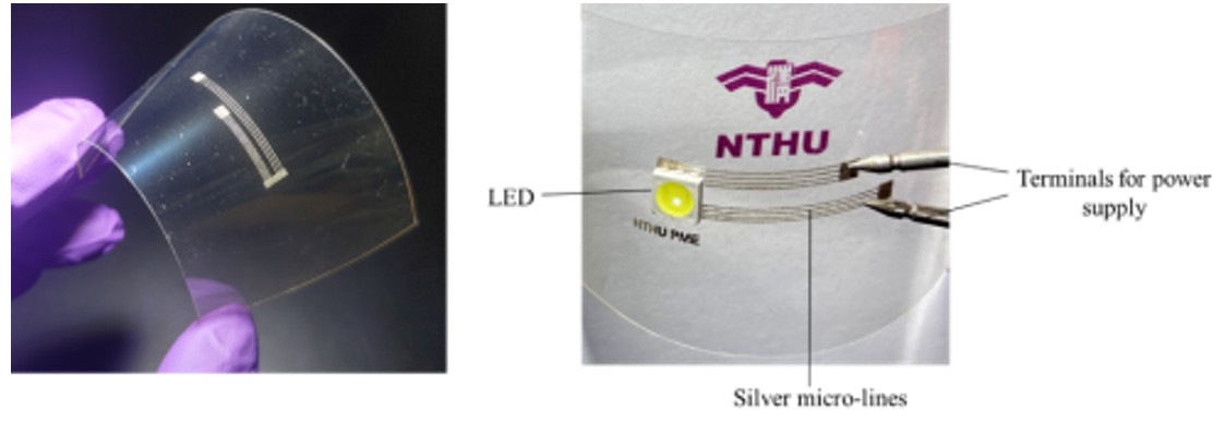
Figure 2. Conductive patterns fabricated by LDSP on a polyethylene terephthalate film for illustration and the demonstration of electrical conductivity. (courtesy of MT Lee’s group at NTHU)
A prototyping intelligent LDSP manufacturing system as shown in Figure 3 is currently under development with supports from the MOST in Taiwan and from industry. Micro-transport analysis in triple-phases (solid, substrate, reactive liquid and possibly vapor) and mechanics analysis have been carried out to investigate the critical factors of the process. Artificial intelligence in conjunction with machine vision and machine learning are applied to improve the efficiency of the process. Equipped with domain knowledge and advanced intelligence technologies, the LDSP is hopefully a green and smart solution to the next generation manufacturing technology for flexible and wearable electronics.
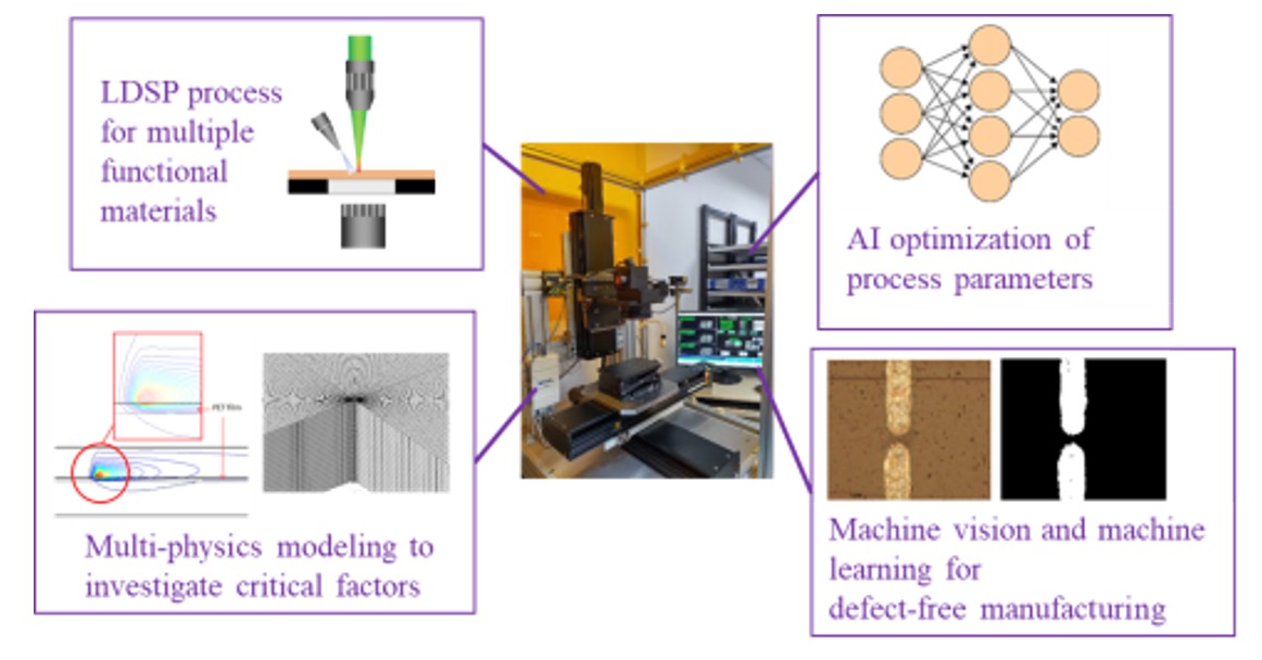
Figure 3. Intelligent LDSP manufacturing system. (courtesy of MT Lee’s group at NTHU)
RELATED
STAY CONNECTED. SUBSCRIBE TO OUR NEWSLETTER.
Add your information below to receive daily updates.