

Using an on-demand, multi-sensor wearable 3D-printed medical device for hemodialysis patient care

Author(s)
K.S. Chang-LiaoBiography
Prof. Chang-Liao has been a professor in the Department of Engineering and System Science in National Tsing Hua University, Taiwan, since 1999. He is a Distinguished Lecturer of IEEE, and he served as the Editor of IEEE Electron Device Letters for the period 2012-15.
Academy/University/Organization
National Tsing Hua UniversitySource
IEEE Electron Device Letters, vol. 40(2), pp. 181-184, 2019.https://ieeexplore.ieee.org/document/8981803-
TAGS
-
Share this article
You are free to share this article under the Attribution 4.0 International license
- ENGINEERING & TECHNOLOGIES
- Text & Image
- April 21,2020
The metal-oxide-semiconductor field-effect-transistor (MOSFET) is the most common semiconductor device in integrated circuits (IC). The process development of channel and gate stack are the key techniques for the high performance MOSFET. A SiGe super-lattice (SL) buried channel was proposed to enhance carrier mobility in MOSFETs. Thus, electrical characteristics of nFinFETs with SiGe and SiGe SL-like buried channels were studied in this work. Results show that the electron mobility of nFinFETs with a SiGe buried channel is enhanced by its SL-like structure. A higher on-state current and on-state/off-state current ratio are also achieved. In addition, a low equivalent-oxide-thickness and a low gate leakage current density in the p-substrate Ge (pGe) MOS device can be simultaneously achieved by a hydrogen plasma (H*) treatment on the GeO2 interfacial layer (IL). It is found that the removal of GeOx with a low oxidation state in GeO2 IL plays a crucial role in the electrical characteristics of the pGe MOS device. Through H* treatment, the electrical and reliability characteristics are improved by GeO2 IL with a high oxidation state. Therefore, a SiGe SL channel and GeO2 IL with H* treatment are promising for high performance Ge MOS devices.
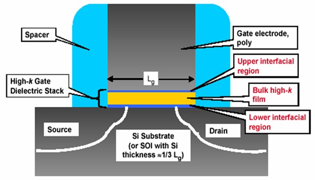
The metal–oxide–semiconductor field-effect transistor (MOSFET) is the most common semiconductor device in digital and analog circuits, and the most common power device. It was the first truly compact transistor that could be miniaturized and mass-produced for a wide range of applications, and its scaling and miniaturization have been driving the rapid exponential growth of integrated ciurcuit (IC) technology. A channel with high carrier mobility and gate dielectric with low equivalent-oxide-thickness (EOT) in MOSFET are required to achieve high performance ICs. Hence, the research and development of channel and gate stack processes are the most crucial works for advanced IC devices.
Fin field effect transistors (FinFETs) have been widely applied beyond conventional planar devices in pursuit of Moore's law. However, carrier mobility is still the most important issue for Si-based FinFET technologies. Since Ge can provide higher carrier mobility than Si, high performance MOSFETs have been achieved by using Si/Ge heterostructure channels. However, the Si/Ge heterostucture channel is rarely applied to FinFET, because its epitaxial growth on the surface of fin is difficult. Recently, some works about the utilization of an epi-SiGe buried channel on MOSFET were reported to improve the on-state current. However, some defects may be generated in the SiGe buried channel if the channel is thicker than its critical thickness. The SiGe super-lattice (SL) structure was proposed as a device channel for MOSFET to obtain a channel with fewer defects and better interface quality because the thickness of each epi-Si/Ge in the SL structure is very thin, and is lower than the critical thickness of epi-Si/Ge. Thus, the carrier mobility of MOSFET can be further improved by the SiGe SL buried channel. The application of the SiGe channel to n-channel MOSFET has rarely been reported, especially for FinFET. Therefore, it is worth studying the effects of the SiGe channel on the electrical characteristics of n-channel FinFET.
Recently, a low equivalent-oxide-thickness (EOT) in an n-substrate Ge (nGe) MOS device was achieved by a post-O2 plasma-oxidation treatment. However, the inevitable growth of the GeO2 interfacial layer (IL) might limit the further scaling of EOT. Besides, the gate leakage current density (JG) would be high as the EOT value scaling reduces to 0.6 nm. A GeOx with low oxidation state has a smaller band-gap (Eg) as compared to GeO2. The smaller Eg may also result in an undesirable increase of JG. On the other hand, it was reported that the interface quality or surface roughness may degrade significantly when no GeO2 IL remains on the Ge substrate surface. Thus, GeO2 IL engineering is the most crucial process to achieve low EOT and leakage current, and to enhance interface quality for pGe MOS devices. Since GeO2 is a thermally unstable material, it is easily degraded into GeOx (1
In summary, devices with a SiGe SL-like buried channel show a higher electron mobility, larger on-state current, and higher ION/IOFF ratio. In addition, the electrical characteristics of the pGe MOS device can be significantly improved by applying H* treatment on the thermally grown GeO2 IL. A low EOT, a low JG, small frequency dispersion, low border trap density, and better device reliability can be simultaneously achieved, while the hysteresis and interface trap characteristics are not affected. Therefore, a SiGe SL channel and H* treatment on GeOx IL are promising for high performance Ge MOS devices.
RELATED


STAY CONNECTED. SUBSCRIBE TO OUR NEWSLETTER.
Add your information below to receive daily updates.